Electronic System Design 3 (ENG3026)
电子系统设计代写 Exam duration: 2 hours to complete exam plus 30 mins for download/upload of submission Attempt any TWO questions
Exam duration: 2 hours to complete exam plus 30 mins for download/upload of submission
Attempt any TWO questions
The numbers in square brackets in the right-hand margin indicate the marks allotted to the part of the question against which the mark is shown. These marks are for guidance only.
Q1
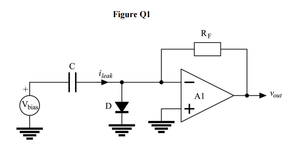
Figure Q1 shows a circuit used to measure the “Time Dependent Dielectric Breakdown” (TDDB) of a silicon MOS capacitor “C”. MOS capacitors are a key semiconductor technology and their lifetime is important. If a large voltage Vbias is applied to a particular MOS capacitor the leakage current ileak is initially small, of order 1 pA. As time goes on the current increases, reaching approximately 100 µA before the capacitor catastrophically breaks down to give currents of order tens of mA. The capacitor may be regarded as a perfect current source for the purposes of analysis at DC.
A1 converts the leakage current ileak to a voltage vout whilst maintaining the voltage at the right-hand side of C to be (ideally) 0 V.
Under normal operation diode D has approximately zero volts across it so that negligible current flows through it when A1 is operating with feedback. When the capacitor C breaks down A1 saturates and D passes the large currents which are flowing, protecting amplifier A1.
(b)
Hence draw the equivalent circuit of Figure Q1 showing all sources of error. [10]
(c)
Hence derive an expression for the total error in the measurement expressed as a current referred to the input. [10]
(d)
A1 is one of the two operational amplifiers listed in the table below.
| Opamp | VOS (µV) | IB (pA) | IOS (pA) | VSupply (V) |
| OPA392 | 10 | 0.9 | 0.9 | ±2.7 |
| ADA4530-1 | 40 | 0.02 | 0.02 | ±8 |
What is the error due to diode leakage for each of these opamps? [4]
(e)
Choose a value of RF for each opamp such that the total input error (including diode leakage current) is three times the diode leakage current in both cases. Note there will be a different value of RF for each opamp. [6]
(f) 电子系统设计代写
i) What is the maximum current ileakwhich each amplifier can measure? (Hint: It is limited by the power supply of the opamps) [4]
ii) Which amplifier gives the widest dynamic range (ratio of largest to smallest detected current)? State the dynamic range in both cases [6]
(g)
If the value of RF was changed to allow for the measurement of a maximum current of 100 µA which opamp gives the smallest detectible current? State the minimum current in both cases [5]
Q2 电子系统设计代写
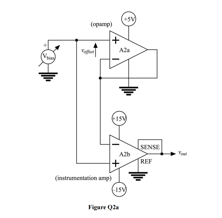
Figure Q2a shows a circuit used to measure the offset voltage of an opamp (A2a, type MCP6291) as a function of input bias voltage, and hence to determine the common-mode rejection ratio of A2a. A2a is a single-supply opamp powered from a single +5 V supply and Vbias is allowed to vary over the full supply range of 0 V to +5 V.
The offset voltage is measured using an instrumentation amplifier A2b which is powered from a conventional split ±15 V supply.
(a)
(i) Draw the diagram of a conventional 3-opamp instrumentation amplifier, indicating the name and tolerance of all resistors used. [6]
(ii) State expressions for the differential voltage gain and common-mode rejection ratio of the input and output stages and hence for the amplifier as a whole. What is the tolerance of the overall differential gain? [6]
(b) 电子系统设计代写
The specified common-mode rejection ratio of A2a is 80 dB minimum and maximum value of offset voltage is 3mV. What value of CMRR must A2b have if the performance of A2a must be characterized accurate to 10% of these values? In other words, what CMRR for the instrumentation amplifier is required to measure an opamp CMRR of 100dB and an opamp offset voltage of 0.3 mV? [5]
(c)
Explain why it is useful for A2b to have as large a voltage gain as possible. Hence specify a suitable gain for A2b for use in characterizing A2a. [8]
(d)
Using your answers to (b) and (c) design A2b being careful to state values and tolerances of all passive components. Quote calculated values, you do not need to use preferred resistor values. [10]
(e)
Explain why the method used to measure the CMRR is different for an opamp relative to the case of an instrumentation amplifier and describe how opamp CMRR is measured in practice. [6]
(f)
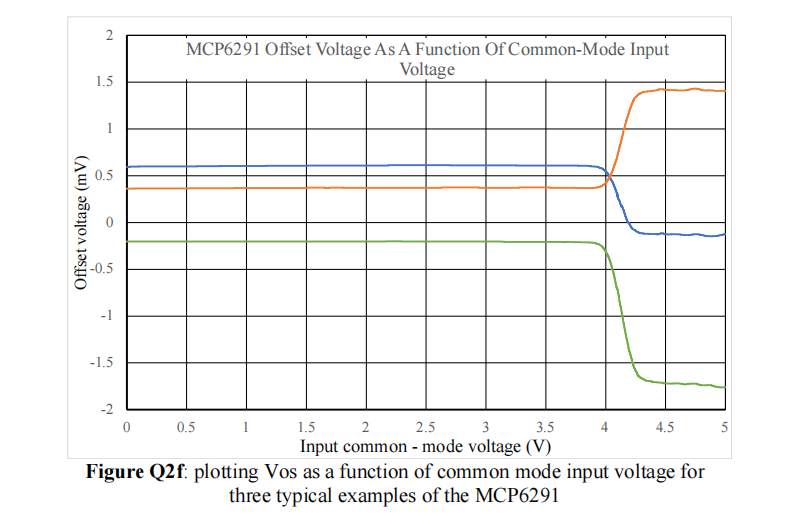
The datasheet for A2a gives typical plots for offset voltage as a function of common mode input voltage which are reproduced in simplified form above in Figure Q2f. Something bad clearly happens between 4 V and 4.25 V input. Calculate the CMRR of these three examples of an MCP6291 over this range. You may refer to them as “orange”, “blue” and “green” respectively. [6]
(g)
Would the A2a give better performance as an inverting amplifier or a noninverting amplifier? Explain why. [3]
Q3 电子系统设计代写
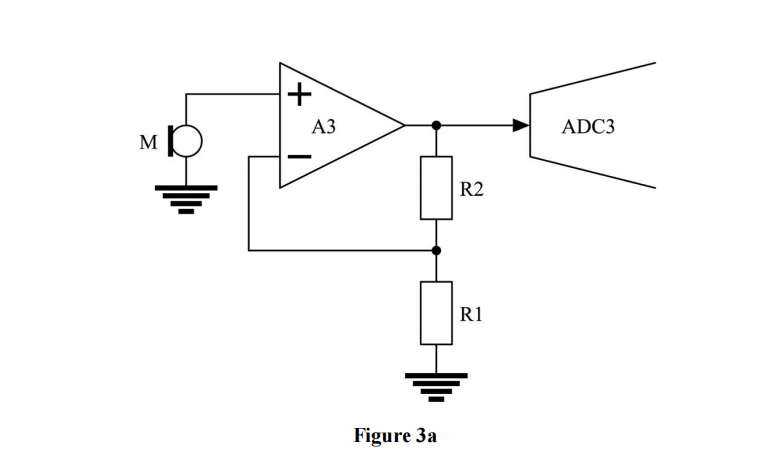
Figure 3a shows an amplifier constructed using opamp A3 which is being used to amplify the output of a microphone M and to drive an analogue to digital converter ADC3.
(a)
Re-draw the figure to include all sources of noise. You do not have to consider any noise sources associated with ADC3 itself and the microphone should be represented by a general Thevenin equivalent voltage source. [10]
(b)
Hence derive an expression for the total input voltage noise spectral density of the amplifier referred to the input [10]
(c) 电子系统设计代写
What is the voltage noise spectral density of the amplifier referred to the output? [3]
(d)
ADC3 is an AD7134 which has a typical input voltage noise amplitude of 1.6 µV RMS at a bandwidth of 162 kHz. Calculate the voltage noise spectral density of the ADC assuming the noise is uniform across the bandwidth (white noise). [3]
(e)
Explain, using a suitable diagram, why the noise performance of an amplifier having both input voltage and current noise is best at a particular value of source resistance, and justify an expression for the optimum source resistance. [7]
(f) 电子系统设计代写
The input to A1 is supplied from a microphone M (Shure SM7B) having source resistance 150 Ω with a maximum output voltage of 280 mV p-p. The maximum input voltage range of the AD7134 is 5V p-p. Choose values of R1 and R2 to give appropriate gain without significantly increasing the noise produced by the amplifier. [4]
(g)
A3 is one of the three amplifiers indicated in the table below. Using your answer to part (e) choose the best amplifier for this application. [3]
| Amplifier | Input voltage noise spectral density nV·Hz-1/2
|
Input current noise spectral density fA·Hz-1/2
|
| AD797 | 0.9 | 2000 |
| OPA827 | 4 | 2.2 |
| ADA4530-1 | 16 | 0.07 |
(h)
(i) Calculate the RMS voltage noise at the output of your amplifier over a bandwidth of 162 kHz. [3]
(ii) What circuit element limits the noise level of your system? [3]
(iii) How many bits of resolution should ADC3 have? [4]