EE4321 Analog Electronics Circuits
Homework Transistor Simulations
模拟电子电路课业代写 Intro:We are using the EE4312_SpiceModel_2021.inc model library for a 0.5um CMOS technology with a supply voltage of 3.0V. You can use any
Intro: 模拟电子电路课业代写
We are using the EE4312_SpiceModel_2021.inc model library for a 0.5um CMOS technology with a supply voltage of 3.0V.
You can use any W >= 1um and L = 0.5um, 1um, 2um, 4um or 8um with the associated model cards given below. The models provided are LEVEL 2 models1 which are simple models, however, they have the benefit that parameters can easily be interpreted. In order to obtain proper output conductances, a different model card is provided for different transistor lengths2 .
1 Much more sophisticated models exist that model the sub-micron effects better and where one model card can be used for different lengths, but we choose to use a simple model that can be easily interpreted for educational reasons.
2 If you need longer transistors, then you will need to add an additional model card to the library with a proper value for the LAMBDA parameter.
You can assume that LDIF = 2*LMIN or 1um. For a simple transistor layout AD = AS = W*LDIF and PS = PD = 2W + 2LDIF.
| L | Model Card NMOS | Model Card PMOS |
| 0.5um | CMOSN_05 | CMOSP_05 |
| 1um | CMOSN_1 | CMOSP_1 |
| 2um | CMOSN_2 | CMOSP_2 |
| 4um | CMOSN_4 | CMOSP_4 |
| 8um | CMOSN_8 | CMOSP_8 |
Assignments: 模拟电子电路课业代写
1.
Simulate the IDS/VGS characteristics of the NMOS and PMOS transistors3 in the table below with VDS = 1.5V using a .DC simulation sweeping VGS from 0V to 3V.
a. Estimate the VT of the transistor (Hint: plot sqrt(IDS) vs VGS and extrapolate the intersection with the VGS axis from the current region of the device operating instrong inversion)
3 The VGS and VDS values used below are for an NMOS transistor; for the PMOS transistors use the appropriate signs. Note that you can set up a single schematic with all the transistors so you can simulate all transistors in one go.
b. Plot the gm of the transistors (Hint: d(id(Mx)) is the derivative dIds/dVGS)
c. Plot the (gm/IDS) of the transistors (Hint: plot d(id(Mx)/IDS)
d. Find the current IDS and gate voltage VGS for which (VGS-VT) = Vov = 200mV, 400mV and 600mV and summarize in a table; review how the current scales with Vov and W/L
e. With an .OP simulation for a Vov = 200mV check that the operating point information reported in terms of Vov and current corresponds your findings above
| Transistor | W | L | W/L |
| M1 | 1u | 0.5u | 2 |
| M2 | 2u | 1u | 2 |
| M3 | 16u | 8u | 2 |
| M4 | 16u | 2u | 8 |
| M5 | 16u | 0.5u | 32 |
2. 模拟电子电路课业代写
Simulate the IDS/VDS characteristics of the NMOS and PMOS transistors with VGS such that Vov = 200mV, 300mV, 400mV, 500mV (Hint: VGS can be calculated based on VT in 1)
a. Check the VDSsat
b. Check the gout (Hint: plot d(id(Mx)) which is the derivative dIds/dVDS)
c. Compare to .OP simulations
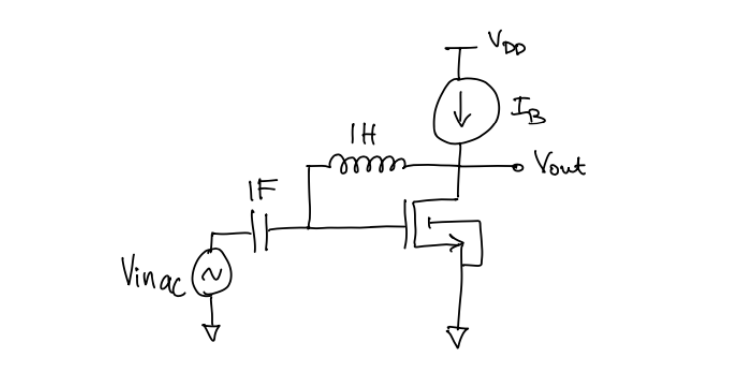
3.
Simulate the gm/gds of the NMOS and PMOS transistors biased with current such that Vov is 200mV and 400mV using the schematic below:

a. Summarize the results in a table
b. Compare simulations against hand calculations based on the small-signalparameters reported by a .OP simulation.
c. Review the gm/gds, gm, and gds scaling with Vov, W/L and L
4.
Simulate the fT ofthe NMOS and PMOS transistors biased with a Vov of 200mV and 400mV for a VDS of 1.5V
a. Summarize the results in a table
b. Compare simulations against hand calculations based on the small-signal parameters reported by a .OP simulation.
c. Review the scaling with Vov, W/L and L