ECSE 2610 Computer Components and Operations
ECSE 2610 – Studio 1
代写计算机组件和操作 Design, implement, and test a 2 bit comparator on Basys 3 board Objective: The objective of this studio is for you to use VHDL to
Design, implement, and test a 2 bit comparator on Basys 3 board
Objective:
The objective of this studio is for you to use VHDL to design a 2-bit comparator and implement it on an FPGA chip on Basys3 board. You will then test proper functionality of the circuit. The FPGA board’s slide switches should be used for inputting two 2-bit numbers, and the comparator outputs, three of them, should be mapped to any three LEDs available on the board.
Discussion:

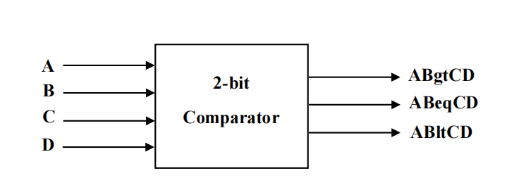
Inputs
The inputs to the 2-bit comparator are A, B, C, and D; shown above. These are binary variables that can each take binary values of ‘0’ or ‘1’.
(N1)10 = (AB)2 Number 1 is AB (A is most significant bit and B is least significant bit of N1)
(N2)10 = (CD)2 Number 2 is CD (C is most significant bit and D is least significant bit of N2)
Each of these four inputs should be controlled using a slide switch on the board.
Outputs
The 2-bit comparator has 3 outputs.
ABgtCD: AB greater than CD (or N1>N2)
ABeqCD: AB equal to CD (or N1=N2)
ABltCD: AB less than CD (or N1<N2)
Each of these outputs should be connected, or mapped, to a LED on the board. Note that these outputs are mutually exclusive.
Entity of Comparator 代写计算机组件和操作
Entity (of a VHDL code) lays out the inputs and outputs of a design and treats everything else as a black box. In other words, in this part of the code you only need to specify the inputs and outputs of your design. The relationship between the outputs and inputs is described in the architecture part of the code.
Just as you did in the Vivado Design Suite tutorial (attached on Piazza), using the wizard during project creation and adding new sources, add the input and output bit entries for comparator.
Important: When choosing directory names, file names or project names, you should avoid starting them with a number. Instead of ‘2bitcomparator’, use ‘comparator_2bit’. Also avoid spaces.
Architecture 代写计算机组件和操作
This part of the code describes the relationship between the outputs and the inputs. For this, you would need to first fill out the truth table below for all the 16 possible combinations.
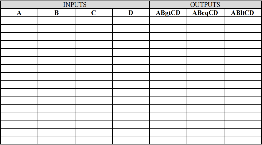
Once the above table is complete, write logic expressions for the three outputs in terms of the inputs. You may choose to simplify these expressions using Boolean algebra properties or other logic simplification techniques that you might know (optional).
The VHDL keywords for logic gates: NOT, AND, OR
Complete the architecture of your design by inserting the logic expressions derived earlier, the signal assignment operator, and the appropriate keywords for the corresponding logic gates.
An example of such signal assignment from the tutorial is C <= A AND B;
Constraints File and Programming into FPGA 代写计算机组件和操作
In the tutorial you mapped the inputs A and B to two switches and the output C to an LED in your Xilinx design constraints file (XDC). Using a similar XDC file creation process, map the inputs, A, B, C, and D to four different slide switches on the board. For the outputs, you may use any three of the LEDs that are located just above the slide switches. To complete writing the XDC file, you need to look at the master constraints file for the board, available on piazza under studio resources, and only include statements that map the 4 inputs and 3 outputs.
Save all your work and work on generating the bitstream (.bit file). Connect the Basys3 board to your windows machine and power it on. Make sure the power select jumper is set to USB. Use the slide switches and LEDs to test your design.
Evaluate and Correct 代写计算机组件和操作
Now you will want to verify that the comparator design works correctly. Change inputs using the slide switches and check whether the correct LED turns on or not for all 16 test cases.
Demonstrate your work to the TA and get checked off. While check off, the TAs may ask you a couple of questions to check your understanding. You will be asked to demonstrate at least 3 test cases.
After you are done with the studio work: Turn off your FPGA board, gently unplug the USB cable from the board and coil it. Place the board in the box with foam padding and keep both the box and cable in a safe place away from food or drinks.
Gradescope submission guideline (valid after TA check off)
Studio 1 write-up should be uploaded to Gradescope. It should include the following deliverables:
- (5 pts) Logic expressions used for ABgtCD, ABeqCD, and ABltCD.
- (5 pts) VHDL code.
- (5 pts) XDC file.
- (5 pts) Explain how you tested your design including the test cases. Note that only a few test cases are required while TA check off but you should test all 16 cases to completely validate your design. Did you get satisfactory result for all 16 cases?
- (5 pts) Summarize your experience for this studio. What was challenging/easy/confusing? Can you think of a different way to design and implement such as comparator? Anything else you would like us to know.