
Analogue Electronics – Coursework 2
模拟电子学报告代写 Filters are frequency selective devices that are used to select desirable band of frequency. As such, filters have low attenuation in the passband
Microwave Low-pass Filter Design 模拟电子学报告代写
The aim of the coursework is to learn how filters in printed circuit technology are designed.
All design is done in the Advanced Design System (ADS) software. Instructions on how to download ADS software on your computer is given separately.
Please note: Support for the coursework is done during lecture engagement slots. For the lab session to be of use to you it is essential that you familiarise yourself in advance with the ADS software.模拟电子学报告代写
Total report should be written in the pre-defined format, submitted as a PDF format and cannot exceed 8 pages.
References
A specific reference for this project is:
David M. Pozar, Microwave Engineering, John Wiley & Sons.
Introduction 模拟电子学报告代写
Filters are frequency selective devices that are used to select desirable band of frequency. As such, filters have low attenuation in the passband and high attenuation in the stopband. Depending on the position of the passband filters can be classified in low-pass (passband from 0 to wc), high pass (passband from wc to µ) and bandpass (passband from wc1 to wc2) filters, where wc denotes the cutoff frequency. Most popular filter characteristics are maximally flat filter (or Butterworth filter) and Chebyshev filter. In this coursework we will base our design on the Butterworth filter response.模拟电子学报告代写
Ideal filters cannot be realised so appropriate specification in terms of insertion loss in the passband and in the stopband needs to be given. For example, in the case of a maximally flat low-pass prototype filter specification includes defining the maximum insertion loss in the passband (ILmax), the minimum insertion loss in the stopband (ILmin), and the cut-off frequency wc as shown in Fig.1. Please note that x-axis is normalised with the cut-off frequency w/wc. Fig.1 also shows that higher order filters (higher N) more closely approximate ideal filter characteristic.
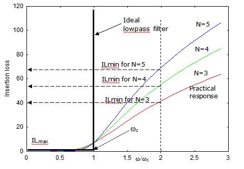
Fig.1. Maximally flat filter characteristics for a low pass prototype filter
This coursework will consider a simple approach in designing a low pass filter – stepped impedance filter. Stepped-impedance filters are popular as they are easy to design and take up less space than low-pass filters using stubs but their performance is not as good due to approximations used in the design process.
Design procedure of a stepped-impedance microwave filter goes through 5 steps and these are:
STEP1: Defining filter characteristics.
These parameters will be defined for you and they include:
a.Insertion loss (IL) in the passband. The passband is defined by a cutoff or pass-band frequency wc. In the case of a lowpass filter the passband is from 0- wc.
b.Minimal insertion loss at the frequency ws– this frequency characterizes the edge of the stopband. The insertion loss in the stopband is required to be greater than insertion loss at frequency ws.模拟电子学报告代写
c.Input and output impedance of the system. This is usually 50W
Not every filter will satisfy given filter characteristics, and therefore, based on given filter characteristics the order of the filter is first found. The appropriate order of the filter, N, is determined for given filter specifications. For the maximally flat filter characteristic the order of the filter that satisfies given filter characteristics is given by:
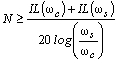 (1)
(1)
STEP 2: Select appropriate lowpass prototype filter
Lowpass prototype filter is a lumped element circuit operating at 1 W impedance system with a cut-off frequency of w=1rad/s. The elements of the lowpass prototype filter are pre-calculated and are given in the Table 1 in Part B for filter orders N=1,..9. based on your calculation of eq(1) you will select appropriate filter order from Table 1 and determine normalised values for source impedance and load, and circuit capacitances and inductances (g1, …g10).模拟电子学报告代写
STEP 3: Transformation of the low-pass prototype network into the microwave LC filter network.
This includes scaling the lumped circuit elements to 50W load impedance system. The frequency of the prototype filter is also scaled from w=1rad/s to a desired wc=2pfc. These transformations are called impedance and frequency scaling.
New values of L’, C’ and the source and load impedances (RS, RL) are:
 (2)
(2)
STEP4: Convert the LC microwave filter into transmission line filter.
Lumped element filters are not practical at high frequencies as their size is proportional to the wavelength of the signal and wave effects deteriorate characteristics of the component. Instead, L and C components are converted into equivalent transmission line stubs for which electrical length (bl) and characteristic impedance (Zo) are defined. Transmission lines are idealised representation of practical lines (microstrip, stripline etc) and are characterised by characteristic impedance Zo and electrical length q=bl at a specific frequency. Once we know Zo and q we can determine physical dimensions of transmission lines, in our case microstrip line.模拟电子学报告代写
a)Converting inductors into equivalent transmission lines
An inductor component can be approximated by a transmission line of high characteristic impedance. The transformation is shown in Fig.2 and is achieved by:
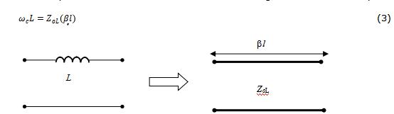
Fig.2. Lumped inductor and equivalent transmission line
For mapping to work we need to decide on 2 parameters: characteristic impedance of the line (ZoL) and electrical length of the line (bl).
Typically, the value of the characteristic impedance ZoL is chosen by a designer. The value of characteristic impedance depends on the technology in which filter is realised (microstrip line or stripline). In the case of microstrip line, high values of the characteristic impedance ensure better mapping. This is however limited by practical fabrication limits as high impedance implies very thin microstrip line. Typically impedance as high as ZoL=120W can be realised in microstrip.模拟电子学报告代写
So it is safe to assume that characteristic impedance is 110 W. The electrical length can be obtained as
![]()
Please note that q is calculated at cut-off frequency wc.
Note: As you increase the characteristic impedance of the transmission line the width of the practical miscrostrip line reduces, so there will be a point at which widths are too narrow and hence difficult to produce using lithography.
b)Converting capacitors into equivalent transmission lines
It can be shown that inductor can be approximated by a transmission line of low characteristic impedance. The transformation is shown in Fig.3 and is achieved by:
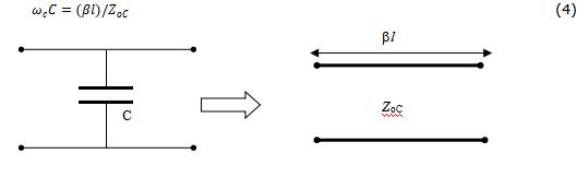
Fig.3. Lumped capacitor and equivalent transmission line
For mapping to work we need to decide on 2 parameters: characteristic impedance of the line (ZoC) and electrical length of the line (bl).
Typically, the value of the characteristic impedance ZoC is set to be low. In the case of microstrip technology, the choice is usually ZoC=30W.模拟电子学报告代写
STEP 5: Converting the transmission line filter into microstrip filter: producing a layout of the filter.
In this section you will use ADS software to obtain physical dimensions of the filter and produce a layout that is ready for fabrication. Based on known characteristic impedance and an electrical length the software outputs the width and the length of a microstrip line specified for a given substrate. The process in which the physical widths and lengths of microstrip lines are obtained is called synthesis. The inverse process, where the characteristic impedance and the electrical length of a physical microstrip transmission line are obtained from the width and length of the microstrip line is called microstrip line analysis.模拟电子学报告代写
The software for microstrip line synthesis is embedded within the Advanced Design System. For a given transmission line (characteristic impedance, electrical length at the cut-off frequency) and for given parameters of the substrate, the ADS software will return widths and lengths of a microstrip line.
DESIGN TASK 模拟电子学报告代写
Following a design approach outlined in the introduction of the coursework, design a maximally flat low-pass filter that has the cut-off frequency at 5 GHz, maximum insertion loss in the passband of 0.5 dB, at least 15dB attenuation at 7 GHz and input and output impedance of 50W. Filter is to be realised in the microstrip circuit technology.
A selected microstrip maximally flat low pass filter will be compared to a Chebyshev microstrip filter of the same order.模拟电子学报告代写
The normalised lowpass prototype filter parameters and the ladder circuit are given in Table 1, Table 2 and Figure 4 respectively.
The input and output filter impedance is 50W. Microstrip substrate material parameters are:
| Substrate thickness | H | 2.5mm |
| Relative dielectric constant | er | 4.2 |
| Relative permeability | Mur | 1 |
| Conductor conductivity | Cond 模拟电子学报告代写 | 105 |
| Cover height | Hu | 10mm |
| Conductor thickness | T | 0mm |
| Dielectric loss tangent | TanD | 0 |
| Conductor surface roughness | Rough | 0mm |
| N | g1 | g2 | g3 | g4 | g5 | g6 | g7 | g8 | g9 | g10 |
| 1 | 2.0 | 1.0 | ||||||||
| 2 | 1.4142 | 1.4142 | 1.0 | |||||||
| 3 | 1.0 | 2.0 | 1.0 | 1.0 | 模拟电子学报告代写 | |||||
| 4 | 0.7654 | 1.8478 | 1.8478 | 0.7654 | 1.0 | |||||
| 5 | 0.6180 | 1.6180 | 2.0 | 1.6180 | 0.6180 | 1.0 | ||||
| 6 | 0.5176 | 1.4142 | 1.9318 | 1.9318 | 1.4142 | 0.5176 | 1.0 | |||
| 7 | 0.4450 | 1.2470 | 1.8019 | 2.0 | 1.8019 | 1.2470 | 0.4450 | 1.0 | ||
| 8 | 0.3902 | 1.1111 | 1.6629 | 1.9615 | 1.9615 | 1.6629 | 1.1111 | 0.3902 | 1.0 | |
| 9 | 0.3473 | 1.0 | 1.5321 | 1.8794 | 2.0 | 1.8794 | 1.5321 | 1.0 | 0.3473 | 1.0 |
Table 1. Element values for maximally flat low pass Filter Prototypes (g0=1, wc=1, N=1 to 9)
| N | g1 | g2 | g3 | g4 | g5 | g6 | g7 | g8 | g9 | g10 |
| 1 | 0.6986 | 1.0 | ||||||||
| 2 | 1.4029 | 0.7071 | 1.9841 | |||||||
| 3 | 1.5963 | 1.0967 | 1.5963 | 1.0 | 模拟电子学报告代写 | |||||
| 4 | 1.6703 | 1.1926 | 2.3661 | 0.8419 | 1.9841 | |||||
| 5 | 1.7058 | 1.2296 | 2.5408 | 1.2296 | 1.7058 | 1.0 | ||||
| 6 | 1.7254 | 1.2479 | 2.6064 | 1.3137 | 2.4758 | 0.8696 | 1.9841 | |||
| 7 | 1.7372 | 1.2583 | 2.6381 | 1.3444 | 2.6381 | 1.2583 | 1.7372 | 1.0 | ||
| 8 | 1.7451 | 1.2647 | 2.6564 | 1.3590 | 2.6964 | 1.3389 | 2.5093 | 0.8796 | 1.9841 | |
| 9 | 1.7504 | 1.2690 | 2.6678 | 1.3673 | 2.7239 | 1.3673 | 2.6678 | 1.2690 | 1.7504 | 1.0 |
Table 2. Element values for equal-ripple low pass filter prototype (g0=1, wc=1, N=1 to 9)
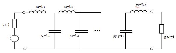
Fig.6. Ladder circuit for low pass prototype and their element definitions
ADS Licenses
You can get a 12 month student license for the Keysight (formerly Agilent) ADS software so that you can install it on your laptop or home computer. ADS is available for Windows and Linux. If you cannot install the software on your own PC for any reason, you will be able to complete the assignments in the engineering computer labs, rather than at home on your own PC. Think of the ability to download and install the software on your own PC as a bonus, rather than an essential requirement or a right. You are advised to get Version 2015.01 (this is what you will find in the engineering computer labs).模拟电子学报告代写
GETTING YOUR OWN ADS LICENSE
- Go to the Keysight web site (http://keysight.com/find/eesof-university)
- Click on Resources for Students
- Under the heading Student Licenses, click the link that says Student License Request Form
- Choose Europe as the region from where you are applying
- Use the information below to fill out the form (the fields not listed belowwill need your personal information entering):
University Name: University of Nottingham
University Address 1: University Park
University Address 2: Electrical and Electronic Eng 模拟电子学报告代写
City: Nottingham
Post code: NG7 2RD
Country: United Kingdom
Business Phone: 01157486158
Business Phone: steve.bull@nottingham.ac.uk
Professor Name: Dr S Bull
Professor Email Address: steve.bull@nottingham.ac.uk 模拟电子学报告代写
- As it explains on the page, you will need to enter the host ID of your PC to fix the license to that machine – To get the host ID (of your laptop/home PC) you will need to EITHER run a JAVA script, as it says on the web page; OR the “host ID” is just your MAC address without the dashes.You can find your MAC address on a Windows PC by opening a cmd window and entering the command “ipconfig/all” The bit you are looking for is “Physical Address”, a series of hexadecimal numbers. Enter this number WITHOUT THE DASHES, e.g. 00-0E-25-F3-BC-25 would be 000E25F3BC25
- You are advised to get Version 2015.01(this is what you will find in the engineering computer labs).

其他代写:program代写 cs作业代写 app代写 Programming代写 homework代写 考试助攻 finance代写 代写CS finance代写 java代写 course代写 report代写